vlsi project
Digital Multiplying Delay Locked Loop
DMDLL
Introduction
The DLL is used for many clock alignment applications, including on-chip clock generation, high speed serial I/O links, and clock recovery circuits in communication systems. This clock alignment function can be provided by either phase-locked loops (PLL) or delay-locked loops (DLL). Some advantages of the DLL include unconditional stability, low phase-error accumulation, low sensitivity to supply noise or substrate noise, and a fast locking time. But the traditional DLL has a major drawback in that, unlike a PLL, it is incapable of frequency multiplication.
Multiplying DLL architectures can overcome this drawback while keeping the merits of the traditional DLL. Although this digital MDLL uses more area and power than an analog MDLL, its design has better portability and scalability. We are proposing an implementation of a DLL with an operating range from 50MHz to 100MHz in 0.5 um technology.
More details
250Mbps Serializer/Deserializer
The use of serializer/deserializers (SERDES) allows digital data buses to be transmitted over single data lines with embedded clock information, and then recover the data and the clock for further processing. This recovery operation is performed using a delay-locked loop (DLL). For data recovery, where clocks are often sent alongside the data, frequency synthesis is not necessary, and the added complexity of a PLL does not warrant the cost. DLL’s are often much better suited for data recovery due to their inherent stability, lower area, and simpler design constraints.
As technology continues to advance, high speed serial links will become increasingly important. With this in mind, we propose to implement a SERDES which is capable of both transmitting and receiving serial data at a maximum bit rate of 250Mbps. It is also important to consider the method by which data will be transmitted over long data links. Impedance matches will be done off-chip, and differential current-mode drivers have been designed and implemented on chip in the interest of noise immunity and simplicity
More details
Smart Processor
16 – Bit 2 Stage Pipelined MIPS Microprocessor
implemented a simplified 16-bit, 2 stage pipelined MIPS RISC Microprocessor. We have 16 instructions and 16 general purpose registers, with register 0 always 0. Register file is 2 port read and one port write. Same pins are used for memory in/out with multiplexing done by mem_write_enable_s1. Processor is timed using 2 phase non overlapped clocking scheme. Microprocessor directly communicates only with external memory
More details
VHDL/VERILOG MODEL OF A research1451.2
In this projectaper, research 1451 Standards are considered. Nowadays, some vendors supply smart sensors adherent to research1451.2, the standard part that describes Smart Transducer Interface Module (STIM), Transducer Electronic DataSheet (TEDS), and Transducer Independent Interface (TII). Generally, these sensors have a microprocessor-centered architecture, where the CPU is devoted both to handle sensing element signal and to support research1451.2 structure .However, it is said that few commercial products (e.g., Telemonitor TMI931A) are currently supporting research1451.2 because of its relatively high cost; actually vendors prefer research1451.4 , a simpler and cheaper standard solution. It is suitable for analog transducers (e.g., ENDEVCO i-TEDS accelerometers), since it defines only TEDS and requires a small number of additional components. In order to obtain a fast and more compact system, the systemon-chip (SoC) approach can be pursued; C (microcontroller), conditioning electronics, and even sensors can be integrated in one chip, reducing overall cost and simplifying assembly procedures .
New sensors are required to be small, cheap, and smart. This project deals with intelligent sensors embedded in a single chip: a Verilog/VHDL model of an research1451.2 Smart Sensor is proposed to obtain a portable STIM block suitable for customizable compact solutions and allowing low-cost, large-scale production. In order to evaluate performances of the proposed model, working prototypes have been built and some tests have been carried out in a real case (chemical detection sensors). The proposed Verilog/VHDL model has been compared with traditional, software-based, microcontroller solutions showing that a timing performance improvement greater than 50% can be obtained. Finally, to exemplify effectiveness of a portable VHDL model, a single-chip sensor with USB interface and integrated research1451 structures has been realized and experimentally characterized.
Project 1, Inverter
Project 2, XNOR Gates
Project 3, Comparitor
Project 4, Incrementer, Counter
Project 5, Digital to PWM Analog Converter
VHDL Examples
HDL (Hardware Description Language) based design has established itself as the modern approach to design of digital systems, with VHDL (VHSIC Hardware Description Language) and Verilog HDL being the two dominant HDLs.
examples have been simulated by Aldec ActiveHDL Simulator and Synopsys Design Analyzer, as well as synthesized with Synopsys Design Compiler . Several sequential design examples have been successfully tested on Xilinx Foundation Software and FPGA/CPLD board.
Driver
Behavior Code
Behavior Simulation
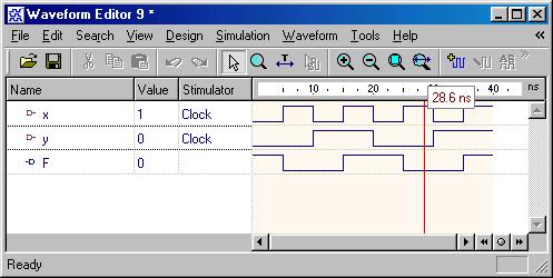
Inverter
Behavior Code
Behavior Simulation
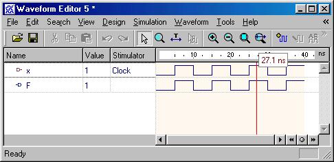
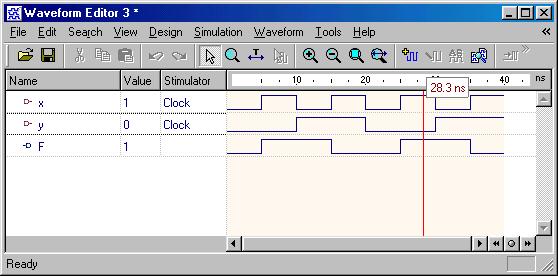
gate
Behavior Code
Behavior Simulation
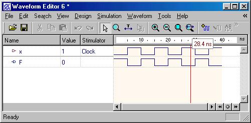
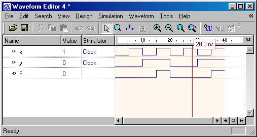
NOR gate
Behavior Code
Behavior Simulation
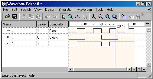
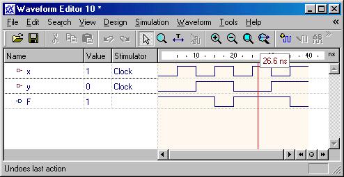
AND gate
Behavior Code
Behavior Simulation
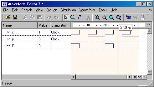
NAND gate
Behavior Code
Behavior Simulation
XOR gate
Behavior Code
Behavior Simulation
XNOR gate
Behavior Code
Behavior Simulation
VLSI project ideas
LDPC Coder/Decoder
On-Chip Security monitors
Physical Random Function generation with Soft Errors
Register file and SRAM
Parity prediction in adders
Multi-sampling latches
On-Chip Bus design
Low-power multiplier